

Context
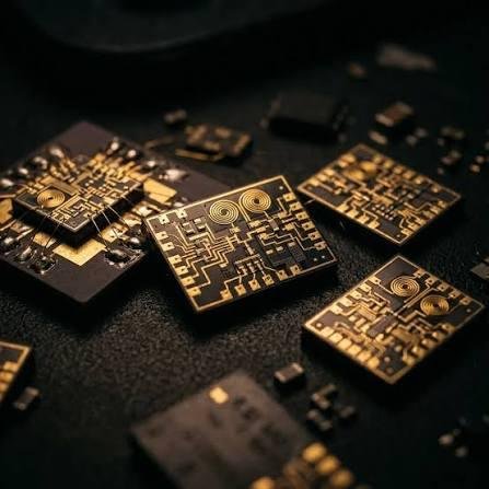
- The Defence Research and Development Organisation (DRDO) has demonstrated and implemented indigenous Gallium Nitride Monolithic Microwave Integrated Circuit (GaN MMIC) technology for advanced defence electronics.
- The technology supports high-frequency systems used in radars, electronic warfare, communications and surveillance.
- Its significance lies not merely in developing another semiconductor chip, but in building indigenous capability in a class of high-power radio-frequency electronics that is strategically sensitive and difficult to import freely.
What Is GaN MMIC Technology?
GaN MMIC technology combines two concepts:
Gallium Nitride (GaN)
- GaN is a wide-bandgap semiconductor capable of operating at high voltage, temperature and frequency.
- These properties allow GaN devices to handle much greater power density than conventional silicon-based electronics.
Monolithic Microwave Integrated Circuit (MMIC)
- An MMIC is a chip designed to process radio-frequency and microwave signals.
- Components such as:
- transistors;
- amplifiers;
- switches;
- resistors;
- capacitors
are fabricated on a single semiconductor platform.
How Does It Work?
A simplified signal chain is:
Weak RF/microwave signal → GaN transistor amplification → High-power output → Radar/EW/communication function
DRDO uses GaN High Electron Mobility Transistors (HEMTs) as key active devices.
A HEMT allows electrons to move efficiently through a specially engineered semiconductor structure, enabling:
- high-frequency switching;
- high-power amplification;
- lower energy loss.
GaN is often fabricated on Silicon Carbide (SiC) because SiC conducts heat efficiently and improves device reliability
What Has DRDO Demonstrated?
DRDO has developed indigenous GaN-based MMICs such as:
- power amplifiers;
- low-noise amplifiers;
- RF switches.
These have been demonstrated for applications extending up to the X-band.
An indigenous GaN chip measuring about 3.5 × 3 mm has reportedly delivered up to 30 watts of power.
DRDO has also developed:
- 4-inch SiC wafers;
- GaN HEMTs;
- GaN MMICs for high-power microwave applications.
The achievement indicates progress across the chain from semiconductor material to operational RF devices.
Why Is GaN Technologically Distinctive?
High power density
GaN can generate greater RF power from a smaller device.
Implication: Radar and electronic-warfare transmitters can become more compact without sacrificing output.
High-frequency performance
GaN operates efficiently at microwave frequencies.
Implication: It supports modern high-resolution radars, secure communications and advanced RF sensing.
Better heat tolerance
GaN-on-SiC devices can operate under high thermal stress.
Implication: Electronics become more reliable in aircraft, missiles, satellites and other harsh operational environments.
Higher efficiency
More electrical energy can be converted into useful RF output.
Implication: Systems require less power and cooling, reducing overall size and weight.
Major Defence Applications
Radar Systems
GaN power amplifiers can generate stronger RF signals, improving detection, tracking and resolution.
Electronic Warfare
High-power RF devices support jamming, signal disruption and threat detection.
Missile and Airborne Systems
Compact electronics can support seekers, guidance, communication and sensing while reducing payload weight.
Satellite and Space Systems
High efficiency and compactness are valuable where power, mass and thermal management are constrained.
Unmanned Platforms
GaN-based communication and sensing modules can improve surveillance and data-link capability in drones and autonomous systems.
Why Does Indigenous GaN Capability Matter for India?
Strategic technology sovereignty
High-end RF semiconductors can be subject to export restrictions. Indigenous GaN capability reduces vulnerability to external denial of critical components.
Defence supply-chain resilience
Domestic production allows radars and EW systems to be repaired, upgraded and replenished without depending entirely on foreign vendors.
Higher indigenous content
India can move from importing complete RF modules towards designing and manufacturing critical components within the country.
Technology absorption
Mastering GaN MMIC fabrication builds knowledge in materials science, wafer processing, device design, packaging and RF engineering.
Dual-use industrial spillovers
The same capability can support:
- satellite communication;
- telecom infrastructure;
- high-power electronics;
- electric mobility;
- advanced sensing.
Key Challenges
- Low manufacturing yield: Advanced GaN fabrication requires extremely precise processes; low yield can increase cost.
- Packaging bottleneck: High-power chips need sophisticated thermal packaging before deployment in operational systems.
- Supply-chain dependence: Substrates, fabrication equipment and specialised materials may still have external dependencies.
- Scale gap: Limited production capability must evolve into reliable industrial-scale manufacturing.
Way Forward
- Improve fabrication yield: Strengthen process control and domestic semiconductor manufacturing capability.
- Build packaging capacity: Develop indigenous high-performance thermal packaging and testing facilities.
- Deepen supply chains: Localise substrates, materials, equipment servicing and critical components wherever feasible.
- Accelerate industry transfer: Move DRDO-developed technology into sustained production through public-private manufacturing partnerships.
FAQs
Q1. What is Gallium Nitride?
GaN is a wide-bandgap semiconductor suited for high-power and high-frequency electronics.
Q2. What is an MMIC?
A Monolithic Microwave Integrated Circuit integrates microwave-frequency electronic functions on a single chip.
Q3. Why is GaN preferred over conventional silicon in defence electronics?
It can handle higher power, higher frequency and greater thermal stress in a smaller device.
Q4. What is a GaN HEMT?
It is a High Electron Mobility Transistor designed for efficient high-frequency and high-power operation.
Q5. Why is indigenous GaN MMIC capability strategically important for India?
It reduces dependence on imported sensitive RF technologies and strengthens domestic capability in radar, electronic warfare and advanced defence electronics.