Important questions for UPSC Pre/ Mains/ Interview:
|
Context
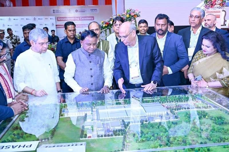
India has taken a major step in semiconductor advancement with the launch of its first 3D glass chip packaging unit in Odisha under the India Semiconductor Mission (ISM).
Q1. What are semiconductors, and why are they critical for modern technology and strategic sectors?
- Semiconductors are materials (mainly silicon) that conduct electricity under controlled conditions.
- They form the basis of integrated circuits (chips) used in all electronic devices.
- Applications include smartphones, computers, automobiles, defence systems and satellites.
- Countries with semiconductor capabilities gain technological leadership, economic strength and strategic autonomy.
Q2. What is Moore’s Law, and why is the semiconductor industry moving beyond it?
- Moore’s Law (1965) states that the number of transistors on a chip doubles every two years, improving performance and reducing cost.
- It drove decades of miniaturisation and efficiency gains in computing.
- However, chips are now reaching physical and thermal limits, making further shrinking difficult.
- This has led to alternative approaches like advanced packaging, chiplets, and 3D integration.
Q3. How do traditional silicon chips differ from advanced 3D glass semiconductor chips?
- Traditional chips:
- Built on flat (2D) silicon wafers
- Components arranged side-by-side
- Limited by space, heat and signal interference
- 3D glass chips:
- Use vertical stacking (3D architecture) like a skyscraper
- Allow higher density and performance within the same area
- Represent a shift from scaling → integration-based innovation
Q4. What are the key features and advantages of 3D glass semiconductor technology and 3DHI modules?
- Uses glass substrates instead of silicon, improving performance.
- Better thermal stability — handles heat more efficiently.
- Lower signal loss — improves speed and reliability.
- Enables high precision and advanced chip design nodes.
- Supports 3D Heterogeneous Integration (3DHI):
- Combines logic, memory, and sensors in one package
- Leads to faster AI processing, efficient data centres, and advanced defence electronics.
Q5. What are the key features of the Odisha 3D glass semiconductor facility and its strategic significance?
- Location: Bhubaneswar, Odisha
- Cost: ₹1,934 crore
- Lead company: 3D Glass Solutions (USA)
- Investors: Intel, Lockheed Martin, and global funds
- Technology: 3D glass chip packaging and 3DHI modules
- Applications: AI, 5G, defence, data centres
- It is the only advanced packaging project among ISM-approved units, making it strategically unique.
Q6. What is the India Semiconductor Mission (ISM), and what progress has been made so far?
- ISM (2021) is India’s initiative to build a complete semiconductor ecosystem.
- Outlay: ₹76,000 crore
- Covers fabrication, packaging, testing, design, and display manufacturing.
- Achievements:
- 10 projects approved across six states
- Investments exceeding ₹1.6 lakh crore
- Includes Tata fabrication plant and Micron OSAT units
- India currently has stronger OSAT (assembly and testing) capacity than fabrication.
Q7. What are the future implications, challenges, and way forward for India’s semiconductor ecosystem?
- Implications
- Positions India in cutting-edge chip packaging technologies.
- Reduces dependence on imports from Taiwan and China.
- Enhances strategic autonomy and supply chain resilience.
- Strengthens India’s role in global tech and defence ecosystems.
- Challenges
- Limited domestic fabrication capacity.
- Need for skilled workforce and advanced infrastructure.
- High capital and energy requirements.
- Dependence on global supply chains for raw materials and equipment.
- Way Forward
- Implement ISM 2.0 with ecosystem-wide focus (~$11 billion planned).
- Invest in skill development and innovation ecosystems.
- Promote public-private partnerships and global collaborations.
- Strengthen semiconductor supply chains and R&D capabilities.
Conclusion
India’s entry into 3D semiconductor technology marks a shift from basic assembly to advanced innovation. Sustained policy support and ecosystem development will be key to achieving technological self-reliance and global competitiveness.